How to Choose the Right GPU Thermal Pad Thickness? Gap Measurement, Compressed Thickness & VRAM/VRM Contact Diagnosis Guide
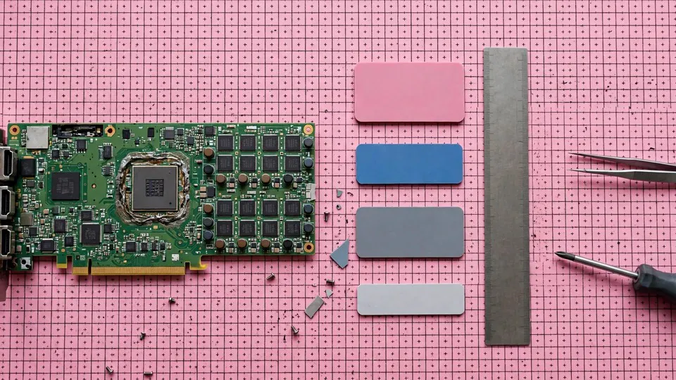
Key Takeaways
Choosing a thermal pad is a contact problem before it is a conductivity problem: each zone needs a pad slightly thicker than its own measured gap, verified by a compressed imprint, so the cooler seats flat on the GPU die instead of being propped up by one over-thick zone.
What Thickness Actually Does
A thermal pad is a gap filler, not a paste. On a graphics card, the GPU die is normally in near-direct contact with the cooler through paste, while VRAM chips, VRM MOSFETs, chokes or inductors, and other parts sit at different heights beneath the same heatsink, cold plate, or backplate. The pad must bridge each individual gap: from the top of the component to the surface of the heatsink above it. If that bridge is incomplete, heat has nowhere useful to go, however good the pad material is on paper.
Two quantities must not be confused, because confusing them is the root of most thickness errors. Uncompressed, or nominal, thickness is the pad as supplied, for example 1.0 mm, 1.5 mm, or 2.0 mm. It is the number printed on the packet. Compressed thickness, also called bond-line thickness, is the thickness once the cooler is screwed down. This is the thickness heat actually travels through, and the thickness at which contact resistance and datasheet thermal resistance are meaningful. Buying a pad by its packet number and assuming that number is the working thickness ignores the whole point of the fitting.
The basic through-plane relation used in engineering guides is that thermal resistance is approximately equal to compressed thickness divided by conductivity multiplied by area. That is why, for the same material and with full contact, a thinner compressed layer is better. But the condition matters more than the conclusion: only if contact is complete. An air void is far worse than a slightly thicker pad, because air is a poor conductor. A pad that is a fraction thicker than necessary but makes full, even contact will usually outperform a pad that is theoretically thinner but leaves part of a chip untouched. Thickness choice is therefore a contact problem first and a conductivity problem second.
Compression ratio is defined as uncompressed thickness minus compressed thickness, divided by uncompressed thickness. A worked example from vendor sizing tables makes the point clearly: a 2.0 mm pad compressed to 1.6 mm is 20 percent compression, and a 1.5 mm pad compressed to 1.2 mm is also 20 percent compression. The same percentage means a different absolute amount of squash on different nominal thicknesses, so percentage alone does not select a pad. The measured gap does. A percentage is a check on a choice already made from a measurement, not a substitute for the measurement.
Hardness governs how much force is needed to reach a given compression and how well the pad conforms to an uneven surface. For graphics cards and mainboards, technical guides converge on soft pads, roughly Shore 00 25 to 70, with softer pads around Shore 00 25 to 50 for uneven surfaces, larger gaps, and sensitive parts such as VRAM chips and MOSFETs, and firmer pads around Shore 00 50 to 70 for flatter surfaces and gaps of about 1 mm or less. Two cautions belong with any hardness number. First, Shore 00 and Shore A are different scales, and a number without its scale is meaningless. Do not compare a Shore 30 figure from one vendor with a Shore 30 figure from another unless the scale matches. Second, a soft pad forgives a small oversize in a way a firm pad does not. The same nominal thickness in a soft pad and in a firm pad can therefore behave differently under the same cooler, which is one reason community thickness tables disagree between card revisions and pad brands. Hardness is part of the selection, not a footnote to it.
Why One Thickness Cannot Fit the Whole Card
VRAM, VRM stages, chokes, and backplate zones sit at different heights and face different heatsink features: a flat plate in one place, a recessed pocket in another, a fin stack in a third. A single thickness can be simultaneously too thin for one zone, leaving no contact, and too thick for another, lifting the cooler. The cooler is a single rigid assembly, so one over-thick zone props it up and unloads its neighbours. In the worst case it unloads the GPU die itself. That is the mechanism behind the classic failure mode in which VRAM temperatures improve after a pad change while core temperatures rise: the new pads are not necessarily poor material, the cooler is no longer seating flat. It is a mechanical seating problem, and treating it as a material problem leads to buying another set of pads and repeating the error.
VRAM and VRM contact differ in ways that matter for selection. VRAM chips are usually a repeated, relatively uniform array around the die, often sharing one flat cooler surface. Height variation between chips is small but not zero, and tolerance stack-up across chip height, solder, PCB flatness, and cooler flatness still matters. VRM parts are mixed: MOSFETs have flat tops and are often the critical contact, chokes or inductors are taller with rounded or uneven tops and are sometimes not intended to be the primary contact surface on every design, and capacitors may only need clearance rather than a pad at all. Treating a choke like a VRAM chip, with the same thickness and the same expectation of flat contact, is a category error. Backplate pads are a separate zone again: the gap to a backplate is typically larger and the thermal path is longer, so backplate thickness cannot be copied from the front-side VRAM thickness. Any selection that is not per-zone is guessing for at least one zone.
Reading Symptoms as Mechanical Evidence
Temperature alone never proves a thickness error. A thickness claim needs a mechanical correlate: an imprint, a measured gap, or a before-and-after change when only thickness changed. The table below pairs common observations with the test that separates one cause from another. In every row, change one variable at a time; changing thickness, paste, and fan settings together destroys the evidence.
| Symptom or observation | Test, changing one variable at a time | Interpretation |
|---|---|---|
| One VRAM zone hot while the rest is normal, or a single chip hotter than its neighbours | Re-open and inspect the compressed imprint on that pad: full and even, faint or absent, or crushed through | Faint or absent means too thin, or unloaded by a neighbouring over-thick pad. An even mark with continued heat means thickness may be right and the cause lies elsewhere |
| Core temperature rises after a pad change while VRAM improves | Inspect GPU-die paste spread and cooler seating on re-opening, and compare with core behaviour before the change where known | Paste spread thin or absent in the centre, or a cooler that rocks, points to the cooler being propped up by over-thick pads, not to a core fault |
| All VRAM and VRM zones hot while the core is normal | Inspect imprints across all zones, and check fan behaviour and airflow separately | Uniformly faint imprints suggest systematically too thin pads or uneven cooler torque. Uniformly good imprints mean looking beyond pads |
| PCB visibly bowed, or cooler screws cannot be fully seated without unusual force | Stop, re-measure, and do not force the screws down | Over-thick or too-firm pads, or a pad placed where the design intended clearance. Forcing risks board and component damage |
| Temperatures unchanged after a pad change | Verify imprints and confirm the old pads were actually the limiting factor | Correct thickness with no change means the bottleneck was not pad contact. Do not keep going thicker in search of a result |
| Pad crumbles, tears, or leaves residue on removal | Note the material state, not just the thickness | Degraded material can mimic a thickness problem through loss of height and contact. Replacement thickness still has to be measured, not copied from the degraded remnant |
Measuring the Gap: Five Methods and Their Traps
Measuring the old pad works only if the old pad is intact and representative. A pad that has been in service is already compressed, and may be dried out, torn, or permanently deformed, a condition known as compression set, in which it does not spring back to its nominal thickness. Measuring a squashed remnant and buying that number buys the compressed thickness as if it were nominal, which systematically undersizes the replacement. If the old pad is fully squashed flat, community guidance suggests going one available size up, but that is a heuristic, not a measurement, and it must be checked by imprint after fitting. If the card uses thermal putty or gap-filler paste instead of a sheet pad, as some original designs do, there is no sheet to measure at all. Do not invent a sheet thickness from putty residue. The old pad gives a starting hint and a zone-to-zone comparison, showing which zones were thicker than others, not a specification.
A digital caliper or micrometer on the removed pad is cheap and direct, but a caliper jaw compresses a soft pad while measuring it. Light, repeatable touch matters, and a single reading on a soft pad is not a reliable nominal thickness. Measure at several points and on several chips in the same zone, and report a range rather than a single number. Tolerance stack-up means the gap is a distribution, not one figure, and a selection built on one reading pretends otherwise.
The compressed imprint is the most decision-useful test in a repair context, because it tests the assembled stack rather than a drawing. Fit the candidate pad, mount the cooler with a normal screw sequence, remove it, and read the mark left on the pad and on the heatsink side. A full, even imprint means contact across the chip. A faint, edge-only mark means marginal contact. No mark means no contact. A mark crushed through to the backing, or a deep groove accompanied by cooler rocking, means over-compression. Its limits should be stated plainly: it is destructive to that fitting, since a pad should not be re-used after crushing and inspection if it is deformed, and it says nothing about hot-state dimensions, because thermal expansion and board warpage under heat can change the gap from its cold value.
The shim or stack method is diagnostic only, never a permanent fix. Thin metal shims or stacked thin pads can be used temporarily to probe a gap: add known thicknesses until contact is just achieved, then select a single pad of that total nominal thickness. Multiple interfaces add contact resistance between layers, and stacked pads can shift, delaminate, or pump out under thermal cycling. Vendor and community sources agree on this point, including guidance not to stack pads to create thickness. If a stack is used to diagnose, say so and replace it with a single pad. Related tricks, such as sliding folded paper into the gap as a feeler, are rough at best: they measure clearance, not the compressed gap under cooler clamping force, and paper itself compresses.
Pressure-sensitive film and profilometry are the engineering reference. Production guidance uses pressure film or laser profilometry across multiple samples to establish a mean gap and its tolerance. That is the correct method for a manufacturer, and it is not expected in a repair shop; the article should not pretend otherwise. Its value here is conceptual: it explains why a single caliper reading on one card cannot be generalised into a universal table for that model. One card is one sample from a distribution shaped by chip height, solder, board flatness, and cooler flatness.
Sizing: Ranges That Disagree, and How to Use Them Honestly
Sources do not agree on one compression target, and the article must not present one as universal. One vendor guide gives 15 to 30 percent at assembly clamping pressure. Another gives 20 to 50 percent, with the example of a 2.0 mm pad for a 1.5 mm gap, which is 25 percent compression. A third gives 10 to 40 percent as a validation window, with the warning that the pad's own thickness tolerance, typically plus or minus 5 percent nominal in production specification, must be included: the worst case for contact is the largest gap combined with the thinnest pad, and the worst case for over-compression is the smallest gap combined with the thickest pad. Presenting any one of these windows as the rule would misrepresent the evidence.
The practical translation is deliberately modest: aim for a pad slightly thicker than the measured gap, verify by imprint, and prefer a softer pad when the gap is uncertain. The engineering form of the sizing relation is that nominal thickness equals measured gap divided by one minus target compression, checked against the pad maker's compression-deflection curve at the actual mounting pressure, where such a curve exists. Where it does not exist, say so. The gap itself is not a single clean number either: it equals heatsink surface height relative to the PCB minus component top height, plus or minus dimensional tolerances, plus flatness, board warpage, and deformation after torquing. One static cold measurement is a snapshot, and hot-state dimensions can differ. This is why two identical-model cards can legitimately need different thicknesses, and why a forum table for a model is a starting hint, not a specification. Community compilations mix manufacturer specifications, forum reports, and database entries, and they do not always distinguish card revisions. Treat any such table as a hint requiring imprint verification.
Ageing argues for mid-window sizing rather than minimum sizing. Pads lose height over time through compression set, so a thickness that imprints well on day one can lose contact later, especially if it was already at the thin end of its window. A pad chosen at the very bottom of its acceptable range has no margin left for that loss. Conversely, a pad chosen with a large oversize has no margin against propping the cooler. Mid-window sizing, verified by imprint, is the balance between those two failure directions.
Conductivity marketing deserves the same scepticism. A higher W per m-K number measured at a different thickness, pressure, or test method does not guarantee a lower temperature in this card, because test conditions vary and the headline number says nothing about compressed thickness or contact pressure in this assembly. A high-conductivity pad that does not contact, or that is twice as thick as needed, can lose to a lower-conductivity pad that contacts fully at the right compressed thickness. Delivered thermal resistance at compressed thickness and pressure is the meaningful quantity; the headline conductivity alone is not a performance specification, and pads should not be ranked by it alone.
Edge Cases That Change the Answer
Mixed zones on one card are the norm, not the exception. Different zones need different thicknesses, and any selection table must be per-zone, covering VRAM, VRM, choke, and backplate separately, and per card revision, or it should not be presented as a table at all. The same model with a different revision or cooler is a different mechanical stack: manufacturers revise coolers and pad layouts without changing the model name, so a thickness that was right for one revision can be wrong for another.
Putty-versus-pad designs are a related trap. Some cards ship with putty on VRAM and VRM. Replacing putty with a sheet pad of a guessed thickness changes the mechanical stack, and the gap must be measured rather than assumed equal to the putty's settled height. Backplate-only cooling is another: some zones are cooled only through the backplate, or not at all by design, and adding a pad where the design intended an air gap can prop the cooler or remove needed clearance.
A heatsink bow or warped cooler defeats uniform pad selection entirely. A bowed cold plate makes one zone look too thin and the opposite zone look too thick at the same time. No uniform pad choice fixes a bowed plate; the plate is the problem, and pad changes will only move the symptom from one zone to another. Screw sequence and torque belong in the same discussion: uneven tightening unloads one side, and cross-pattern, gradual tightening is part of thickness verification rather than a separate ritual. An imprint taken after uneven tightening proves nothing about the pad, only about the tightening.
When Pad Replacement Alone Cannot Fix Temperatures
Pad thickness is only one link in the cooling chain. If imprints are good and temperatures do not improve, the bottleneck is elsewhere, and that result is diagnostic information rather than a failed pad job. Candidates to consider, without diagnosing by temperature alone, include GPU-die paste contact that is dried, misapplied, or lost because pads prop the cooler; fan failure, blocked fins, dust, or case airflow, since the heatsink cannot reject heat it has collected if air cannot move; a heatsink or vapour-chamber defect or bow; a VRM or VRAM component fault; and a card running beyond its designed power or cooling envelope, since pads transfer heat and do not create cooling capacity.
A further caution concerns the readings themselves. A temperature reported by one sensor, such as a hotspot or junction reading, is not the same quantity as another sensor's reading, and different cards report different sensors. Do not compare readings across models as if they were the same measurement, and do not state a universal safe temperature: safe limits are model- and sensor-specific and must be checked against that card's own specification where available.
Misconceptions to Leave Behind
Thicker is always safer or cooler is incorrect. Beyond the gap, extra thickness adds thermal resistance through a longer path and, worse, props the cooler off the die and neighbouring zones. Over-thick is a failure mode, not a safety margin. Soft pads forgive a small oversize; they do not forgive any oversize.
One thickness fits the whole card is incorrect. Zones differ in height and heatsink geometry, and a single-thickness kit is a convenience product rather than an engineering statement. If a kit claims one thickness for VRAM, VRM, and backplate together, that claim itself is a warning sign.
Measure the old pad and buy exactly that number is mostly incorrect. The old pad is compressed, aged, possibly torn, or putty rather than sheet. Its removed thickness is at or below its original nominal, and measuring a soft pad with a caliper compresses it further. It gives a starting hint and a zone comparison, not a specification, and the choice must be verified by imprint.
Higher W per m-K always wins, whatever the thickness, is incorrect. Delivered thermal resistance depends on compressed thickness, contact resistance, and pressure, not on the headline conductivity alone. A pad that does not contact cannot cool, however impressive its datasheet figure.
Stacking two thin pads is the same as one thick pad is incorrect. Each extra interface adds contact resistance, and stacked pads can shift or degrade under cycling. Stacking is a diagnostic probe, not a permanent build.
If the new pads are right, temperatures must fall is incorrect. Pads only transfer heat to the cooler. If the cooler, fans, airflow, paste contact, or the component itself is the limit, correct pads change nothing measurable, and that result narrows the search rather than proving the pads wrong.
Soft pads are always better because they compress more is an oversimplification. Soft pads conform better and forgive sizing error, but they also deform more, can extrude under sustained pressure, and may not hold thickness where a flat, stable interface is needed. Firmer pads suit flat, tight gaps. Hardness must match the gap geometry, not a softer-is-better slogan.
Stop Points and What to Record Before Seeking Inspection
Stop and re-measure if the PCB visibly bows, if cooler screws cannot be fully seated without unusual force, if a pad has been placed where the design intended clearance, or if a fitting has been crushed through during an imprint check. Do not force screws down, do not crush pads to fit, and do not leave a diagnostic stack in place as a permanent build. Those actions convert a sizing question into board or component damage.
Before seeking inspection, record the card model and revision where known, the zone-by-zone gaps or imprint results, the nominal thickness and hardness scale of each candidate pad, the screw sequence used, and the symptom pattern before and after the change, with only thickness changed between the two observations. That record lets an inspection start from the mechanical evidence rather than from a temperature number alone. For inspection in Hong Kong, the shop is Room 1209, Dali Plaza, Shek Mun. The telephone number is 2186 8010 and the WhatsApp number is 6558 6806.
Frequently Asked Questions
How do I know whether my pad is too thick or too thin?
Use the imprint, not temperature alone. A full, even mark means contact. A faint or absent mark means too thin or unloaded by a neighbouring over-thick pad. A crushed-through mark with cooler rocking, or a core temperature that rises after a pad change while VRAM improves, points to over-thick pads propping the cooler off the die.
Can I just measure the old pad and buy the same thickness?
Only as a starting hint. A used pad is already compressed and may be deformed or dried out, so its removed thickness is at or below its original nominal, and a caliper compresses a soft pad further during measurement. Use it for zone-to-zone comparison, choose a candidate slightly thicker than the measured gap, and verify by imprint.
Why do different guides give different compression percentages?
Because they come from different vendors, materials, and mounting pressures, with windows such as 15 to 30 percent, 20 to 50 percent, and 10 to 40 percent. No single percentage is a universal specification. The pad maker's compression-deflection curve at the actual mounting pressure governs where it exists, and the imprint verifies the result where it does not.
Should every zone on one card use the same pad thickness?
No. VRAM, VRM MOSFETs, chokes, and backplate zones sit at different heights and face different heatsink features. A single thickness can be too thin for one zone and too thick for another, and one over-thick zone can prop the whole cooler up and unload the GPU die.
Is a higher W per m-K rating always the better pad?
No. Delivered thermal resistance depends on compressed thickness, contact resistance, and pressure, not on the headline conductivity alone. A high-rated pad that does not contact, or that is far thicker than needed, can lose to a lower-rated pad that contacts fully at the right compressed thickness.
Can I stack two thin pads to reach the thickness I need?
Only as a temporary diagnostic probe, to find the gap, and then replace the stack with a single pad of that total nominal thickness. As a permanent build, stacked pads add interface resistance and can shift or degrade under thermal cycling. Vendor guidance agrees that stacking should not be used to create thickness permanently.
What if temperatures do not change after fitting correctly sized pads?
Then the bottleneck was probably not pad contact. Check GPU-die paste contact, fan operation, blocked fins and case airflow, heatsink bow or vapour-chamber condition, and whether the component itself or the card's power envelope is the limit. An unchanged result with good imprints is diagnostic information, not a reason to keep going thicker.
Does the same model always need the same pad thickness?
No. Manufacturers revise coolers and pad layouts without changing the model name, and tolerance stack-up across chip height, solder, board flatness, and cooler flatness means two cards of the same model can legitimately need different thicknesses. Forum tables for a model are starting hints, not specifications, and every choice needs imprint verification.
How does pad hardness affect thickness choice?
Hardness governs the force needed to reach a given compression and how well the pad conforms to uneven surfaces. Softer pads suit uneven surfaces and larger gaps, firmer pads suit flat surfaces and tight gaps, but a hardness number is meaningless without its scale, since Shore 00 and Shore A are different scales. The same nominal thickness in a soft and a firm pad can behave differently under the same cooler.
When should I stop adjusting pads and seek inspection?
Stop if the board bows, screws cannot seat without unusual force, a pad sits where clearance was intended, or repeated changes move the symptom between zones without resolving it. Bring the model and revision, zone-by-zone imprint results, pad thickness and hardness details, and the before-and-after symptom pattern with only thickness changed, so inspection starts from mechanical evidence.